

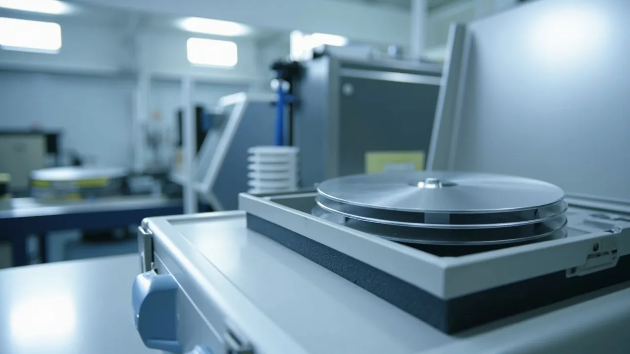
The central conflict in wafer transport is this: a wafer is a thin, high-purity single-crystal slice whose surface tolerates no particles, no metal ion contamination, no electrostatic discharge marks and no micro-cracks, and yet it must survive a real logistics environment with vibration, shock, temperature swings and pressure changes. The short answer: a wafer transport case is not a "crash-resistant box." It is an environmental control system combining cleanliness, micro-vibration control, static dissipation, low humidity and traceability. Acceptance should cover the mechanical interface and cleanliness requirements of the SEMI standards, ISO 14644 cleanroom classes, the ANSI/ESD S20.20 static control framework, and the ISTA / GB/T 4857 transport test methods.
In both front-end and back-end semiconductor operations, wafers move repeatedly: from a wafer fab to an assembly and test facility, from a production line to a metrology tool, from stock to a customer, and from rework back to re-inspection. A 300 mm wafer is high value, large in area and only about 775 micrometres thick. A single instance of poor restraint can cause edge chipping, backside scratches or patterned-layer damage, and most of that damage is invisible on arrival, only showing up after particle inspection or electrical test. For compound semiconductors such as SiC, GaN and GaAs, the material itself is more brittle and warp is more pronounced, which makes transport protection even harder. This article is written for semiconductor process engineers, equipment engineers, clean logistics teams and procurement staff. It covers carrier formats, cleanliness classes, vibration parameters, static control, standards references and an acceptance checklist.
Table of Contents
- 1. Why Wafers Are Hard to Ship: The Triple Constraint of Cleanliness, Micro-Vibration and Static
- 2. Wafer Sizes and Carrier Formats: From 150 mm to 300 mm
- 3. Cleanliness Classes and Particle Control
- 4. Vibration Design: Micro-Vibration, Acceleration Peaks and Resonance Avoidance
- 5. Static Protection: ESD and Wafer Surface Damage Mechanisms
- 6. Humidity, Corrosion and Metal Layer Oxidation Control
- 7. Atmosphere Control: Nitrogen Purge and Low-Humidity Storage
- 8. Inserts and Wafer Racks: Limiting Displacement and Inter-Wafer Friction
- 9. Material Outgassing and AMC Control
- 10. Sealing Levels and the Cleanroom Opening Procedure
- 11. Packaging Hierarchy: Inner Packaging, Outer Packaging and Pallets
- 12. Standards Reference: SEMI, ISO 14644 and the ESD Framework
- 13. Transport Verification: Applying ISTA and GB/T 4857
- 14. Pre-Shipment Inspection and Acceptance Points
- 15. Carrier Cleaning, Refurbishment and Life Management
- 16. Common Misconceptions and Engineering Recommendations
- Frequently Asked Questions
- Conclusion and Further Reading
1. Why Wafers Are Hard to Ship: The Triple Constraint of Cleanliness, Micro-Vibration and Static
Wafer damage mechanisms differ fundamentally from those of ordinary precision parts. Understanding this is the prerequisite for designing a transport case.
Constraint one: cleanliness. Semiconductor yield is extremely sensitive to particles. A sub-micron particle landing on a patterned area can cause a mask defect, a short or an open circuit. Metal ion contamination changes minority carrier lifetime and threshold voltage. During transport, any particle originating from carrier materials, gaskets, inserts or the external environment can become a contamination source. A transport case must therefore not only block particles from outside but also avoid generating particles itself.
Constraint two: micro-vibration. A wafer is a thin plate with relatively low natural frequencies and a pronounced response in certain frequency bands. Sustained vibration during transport causes small displacements within the wafer slots, producing fretting wear at support points and generating particles. For completed patterned layers, sustained micro-vibration can also initiate edge chipping and crack propagation. The damage threshold is far below the "drop" level, which makes this a classic low-amplitude, long-duration failure mode.
Constraint three: static. Wafer surfaces accumulate charge during friction, peeling and gas purging. Discharge leaves local melt marks that destroy patterns. Static also attracts particles, pinning contaminants that would otherwise be carried away by airflow onto the surface. For wafers with protective films, static can also cause film delamination or breakdown.
Two further constraints are secondary but should not be ignored: humidity and corrosion (copper interconnects and metal layers are sensitive to moisture and acidic gases) and pressure change (air freight and high-altitude transport create a pressure differential across the case wall).
These constraints are also coupled. Increasing insert contact area to improve vibration performance may increase particle generation and static accumulation. Increasing the purge rate to improve cleanliness may increase wafer vibration. Designing a wafer transport case is therefore a multi-objective optimisation problem rather than the maximisation of a single metric.
2. Wafer Sizes and Carrier Formats: From 150 mm to 300 mm
Mainstream carrier formats and transport requirements differ substantially by wafer size.
| Wafer size | Common carrier format | Wafer capacity | Cleanliness requirement | Transport characteristics |
|---|---|---|---|---|
| --- | --- | --- | --- | --- |
| 100 / 125 mm | Rack plus hard shell case | 25 per rack | Moderate | Common in compound semiconductor and R and D lines |
| 150 / 200 mm | Open rack plus sealed outer case | 25 per rack | Higher | Mature production lines, equipment spare parts transport |
| 200 mm | Enclosed carrier (SMIF type) | 25 per pod | High | Used in both front-end and metrology steps |
| 300 mm | Front-opening carrier and pod | 25 per pod | Highest | Fully automated handling, fab to assembly and test |
| 300 mm single | Single-wafer shipping box | 1 | Highest | High-value wafers, metrology and rework |
| Large compound semiconductor | Dedicated rack plus custom case | As required | High | SiC and GaN warp heavily, requiring dedicated support |
For 300 mm, the carrier's mechanical interface, such as the door mechanism, locating features and handle positions, must be compatible with the fab's automated handling system. This means the transport case usually does not carry wafers directly. It works in combination with a standard carrier: the standard carrier provides cleanliness and inter-wafer separation, while the transport case provides external shock protection, environmental control and traceability. This hierarchy is a defining feature of semiconductor logistics and is also the point most often confused during selection.
One warning: if the insert of a transport case touches wafers directly, the insert has effectively become the carrier. At that point the insert material must meet semiconductor-grade cleanliness requirements, and ordinary industrial foam is not acceptable. This should be clarified at the concept stage to avoid expensive rework later.
3. Cleanliness Classes and Particle Control
Cleanliness is the top-priority metric for a wafer transport case. The relevant standards framework centres on the ISO 14644 series, covering cleanrooms and associated controlled environments, along with long-established cleanliness classification practice in the semiconductor industry. ISO 14644-1 classifies cleanliness by the permitted particle concentration per unit volume of air, with lower numbers indicating cleaner environments. Critical front-end areas typically operate at very clean classes, and the micro-environment inside a transport case needs to be compatible with them.
Particle control is implemented at three levels.
Level one, source control: material selection for the carrier and insert. The material itself must not be a particle source. Assessment dimensions include whether the material sheds easily, whether it contains migratable low-molecular-weight components, whether it generates wear particles under vibration, and whether the surface is easy to clean. Ordinary EVA, PE foam and injection mouldings often do not satisfy semiconductor requirements, and low-outgassing, low-wear specialty materials are needed instead.
Level two, barrier control: seals and interfaces. Every path between the case interior and the external environment, including the lid joint, breather valve, ports and cable exits, must be a particle barrier. At the same time, interfaces should not carry external particles into the case during opening and closing. Common engineering answers include double-lip seals, labyrinth structures and dust lips outside the sealing face.
Level three, process control: cleaning, packing and opening. Carriers should be cleaned and confirmed before packing, the case should be sealed in a controlled environment, and opening should be performed in a controlled environment with an exterior wipe completed first. Many particle problems do not originate inside the case at all. They come from contamination accumulated on the exterior in an uncontrolled environment and then carried into the clean area.
| Control level | Key measures | Common failure causes | Verification method |
|---|---|---|---|
| --- | --- | --- | --- |
| Source | Low-outgassing low-wear materials, cleanable surfaces | Material shedding, mould release residue | Outgassing testing, wipe sampling |
| Barrier | Double-lip seals, labyrinth structures, dust lips | Gasket ageing, grit embedded in the sealing face | Sealing face inspection, leak testing |
| Process | Cleanroom sealing, exterior wipe before opening | Uncontrolled opening environment, glove contamination | Clean area procedure, sampled particle counting |
4. Vibration Design: Micro-Vibration, Acceleration Peaks and Resonance Avoidance
The vibration control objective for wafer transport differs from general industrial equipment. For general equipment, the question is whether it will be damaged by impact. For wafers, the question is whether long-term micro-vibration will generate particles and edge damage.
Key parameter one: acceleration peak. The acceleration peak experienced by the wafer inside the case should be limited to the range the material and structure can tolerate. In practice this is achieved through a combination of cushion travel and insert stiffness rather than simply adding foam thickness.
Key parameter two: natural frequency and resonance. The packaging system, comprising case, insert, carrier and wafers, is a multi-degree-of-freedom system with several natural frequencies. If a natural frequency falls inside the main energy band of transport vibration, amplitude is significantly amplified. Avoidance measures include adjusting insert stiffness so that system natural frequencies stay clear of the excitation band, adding damping, and avoiding a rigid hard-on-hard connection path.
Key parameter three: number and distribution of contact points. Too few contact points create local stress concentration. Too many create over-constraint, and the wafer cannot expand or contract freely. For 300 mm carriers, inter-wafer location is normally handled by the slots inside the standard carrier, and the transport case only needs to prevent the carrier as a whole from moving.
Key parameter four: constrained directions and degrees of freedom. The carrier should be located inside the case, not clamped rigidly. A practical approach is to locate in three translational directions and limit one rotational direction, leaving elastic allowance in the remaining directions to accommodate dimensional change from temperature.
Key parameter five: drop and shock. Beyond vibration, dropping and shock remain major risks. Cushioning design should cover all six faces and reinforce corners and edges. For single high-value wafers, use an independent cushioning cavity rather than mixing with other items.
For further thinking on cushioning structures, see cushion liner structural design and shock-absorbing sealed case structures.
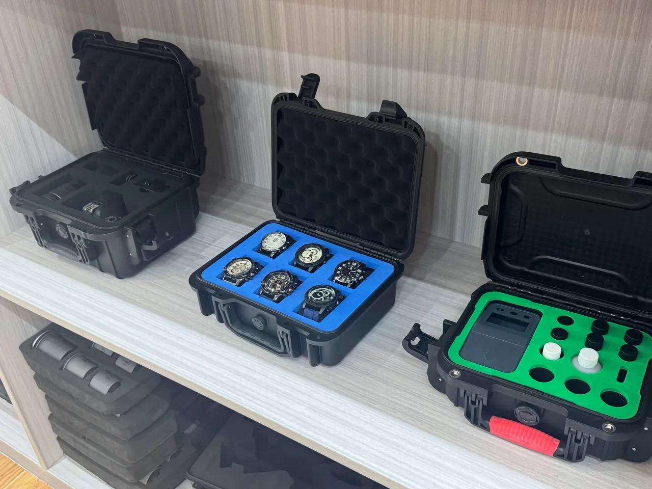
5. Static Protection: ESD and Wafer Surface Damage Mechanisms
The harm static causes to wafers is both hidden and cumulative.
Mechanism one: discharge melt marks. Discharge between charged bodies creates localised high temperature on the wafer surface, melting or vaporising material and producing microscopic point defects or line defects. At specific pattern layers these defects can cause shorts or opens.
Mechanism two: electrostatic attraction. A charged wafer surface attracts airborne particles, pinning contaminants that could otherwise be carried away by airflow, which increases cleaning difficulty and residual risk.
Mechanism three: film damage. For wafers with protective films or coatings, electrostatic discharge can cause film breakdown or local delamination, and can also introduce additional static during subsequent peeling operations.
Static control in engineering practice includes the following.
- Material selection. Materials touching the wafer or carrier should be static-dissipative, and highly insulating materials such as ordinary foam and ordinary plastics should be avoided.
- Grounding path. The carrier, insert and case should be reliably bonded, with a grounding point on the case so that potential can be equalised during handling.
- Operating discipline. Operators should wear antistatic wrist straps and gloves and work at an ESD-protected bench. Lid opening and closing should be smooth to avoid rapid peeling that generates charge.
- Humidity as a supporting measure. Moderately higher ambient humidity helps suppress static accumulation, but it cannot substitute for material and grounding measures, and it must be balanced against low-humidity storage requirements.
The relevant standards framework includes ANSI/ESD S20.20 and IEC 61340-5-1, which respectively address organisational ESD control programmes and the protection requirements for electrostatic-sensitive devices. For structural implementation thinking, see ESD shielding case design.
6. Humidity, Corrosion and Metal Layer Oxidation Control
The harm moisture does to wafers is less like "getting damp" and more like chemical corrosion.
Metal layer corrosion. Copper interconnects, aluminium bond pads and some metal barrier layers corrode when moisture combines with acidic gases such as fluoride or chloride residues and sulphides. The result is pad discolouration, rising contact resistance and reduced solderability. For wafers that have been metallised but not yet packaged, corrosion risk during this transport segment deserves particular attention.
Water marks and adsorption. Water molecules adsorbed on the wafer surface form monolayers and multilayers, affecting downstream processes such as adhesion and bonding, and can leave water marks when temperature changes.
Organic contamination and AMC. Airborne organic molecules and acidic or basic gases, collectively known as airborne molecular contamination (AMC), are adsorbed onto wafer surfaces and form a contamination layer that is difficult to remove. Outgassing from transport case materials is a significant source of internal AMC.
Engineering controls include limiting internal relative humidity, typically with desiccant and a low-humidity environment; using low-outgassing materials; applying an inert gas purge where needed; and fitting humidity indication or logging inside the case. Note that a low-humidity environment increases static accumulation risk, so the humidity target should be set together with static control requirements rather than driven as low as possible.
| Environmental factor | Main risk | Control measures | Metric to balance |
|---|---|---|---|
| --- | --- | --- | --- |
| High relative humidity | Metal layer corrosion, water marks, reduced solderability | Desiccant, sealing, inert gas | Rising static accumulation risk |
| Low relative humidity | Rising ESD risk | Static-dissipative materials, grounding, ionisation | Corrosion risk and low-humidity requirements |
| Organic outgassing | Surface organic contamination, poor bonding | Low-outgassing materials, cleanroom sealing | Material cost and processability |
| Temperature fluctuation | Condensation, dimensional change, film stress | Thermal insulation, cushioning, avoid rapid change | Weight and volume |
| Pressure change | Internal-external differential, seal failure | Pressure equalisation valve, seal design | Cleanliness and airtightness |
7. Atmosphere Control: Nitrogen Purge and Low-Humidity Storage
For high-value wafers or long-term storage, an inert gas purge is a common measure.
Effect of a nitrogen purge. Reducing internal oxygen content and water vapour partial pressure suppresses metal layer oxidation and corrosion, and also slows the oxidation reactions of organic contaminants.
Implementation points. The case needs inlet and outlet ports. Ports should include check valves and quick connectors so that handling does not introduce external contamination. Where the exhaust path could contact the wafer area, it should be filtered. The case interior should be held at slight positive pressure so that any seal defect appears as an outward leak rather than an inward draw.
Why pressure equalisation is necessary. Whether or not inerting is used, a sealed case develops a pressure differential as temperature and ambient pressure change. In air freight, cargo hold pressure is significantly below ground level. Without an equalisation mechanism, the case experiences a large differential that can deform gaskets or stress the structure. A pressure equalisation valve, also called a breather valve, is therefore a critical component of a wafer transport case, and its membrane must simultaneously be hydrophobic, oleophobic and low-outgassing. For selection considerations, see the role and selection of case pressure equalisation valves.
Monitoring oxygen and moisture content. For inerted shipments, fit a re-checkable humidity indicator or logger inside the case and read it before opening. Note that one nitrogen fill does not mean the whole journey is controlled, because inert gas also leaks slowly past sealing faces.
8. Inserts and Wafer Racks: Limiting Displacement and Inter-Wafer Friction
Insert and rack design has two objectives: control each wafer individually and restrain the assembly as a whole.
Per-wafer location. The spacing between wafers is determined by the rack or carrier slots. Slot pitch accuracy, slot profile and support method directly determine how far wafers move under vibration. Slot design should avoid line contact and sharp-corner contact, preferring area contact or large-radius contact.
Whole-assembly restraint. The carrier should have no free space inside the case. A common approach is a bottom locating recess plus a compliant top plate, locating the carrier in all three translational directions.
Avoiding hard points. A locally hard insert concentrates stress during impact and transmits it directly to the carrier and wafers. Insert hardness should be determined by testing rather than taken to the maximum as a matter of habit.
Avoiding cross-contamination. Racks and inserts should be easy to clean, with no difficult-to-reach grooves or blind holes in the structure. Where one case must handle different wafer sizes, this should be achieved by changing the rack rather than the whole case.
Special handling for warped wafers. SiC and GaN typically warp more than silicon. If the support scheme is designed for silicon, support points may float or apply local pressure. Dedicated support surfaces should be designed for the actual warp range and validated with physical samples during the concept phase.
For insert moulding processes and material selection, see custom foam insert solutions and moulding processes and case insert foam material comparison.
9. Material Outgassing and AMC Control
Outgassing is particularly easy to overlook in semiconductor applications. Ordinary industrial plastics, rubbers and foams release trace organic molecules in a closed space. Once adsorbed onto wafer surfaces, these molecules form an organic contamination layer that affects downstream bonding, epitaxy or coating processes.
Material assessment dimensions should include:
- Total organic carbon outgassing tendency: how much organic material the material releases in a closed environment.
- Migratable ion content: migration of chlorine, sodium and potassium causes metal ion contamination.
- Plasticisers and mould release agents: materials containing plasticisers or residual release agents represent a high-risk category.
- Cleaning resistance: the material should withstand the specified cleaning method without degrading or cracking.
- Temperature stability: no significant deformation or release at high transport temperatures or cleaning temperatures.
The engineering recommendation is to treat cleanroom compatibility as the first gate in material selection, not something considered after the structure is frozen. If a material is replaced because it fails cleanliness requirements, tooling usually has to be reworked, which is expensive.
10. Sealing Levels and the Cleanroom Opening Procedure
The IP ratings defined by IEC 60529 and GB/T 4208 need to be reinterpreted in a wafer transport context. The dust digit (6 meaning dust tight) addresses particles entering from outside, while wafer applications also care about particles escaping from inside and about maintaining internal cleanliness. An IP rating is therefore necessary but far from sufficient.
Common configurations are as follows.
| Scenario | Recommended protection | Cleanliness measures | Notes |
|---|---|---|---|
| --- | --- | --- | --- |
| Short transfer inside a cleanroom | IP54 or no sealing requirement | Double bagging plus carrier | Frequent opening, avoid over-sealing |
| Inter-plant road shipment | IP65 | Carrier plus sealed case plus desiccant | Balances protection and handling convenience |
| Air freight or sea freight | IP67 plus pressure equalisation valve | Carrier plus sealed case plus inerting or desiccant | Large pressure and humidity variation |
| Long-term inventory | IP67 plus inerting | Carrier plus sealing plus low humidity plus logging | Requires traceable environmental records |
| Single high-value wafer | IP67 plus independent cavity | Single-wafer shipping box plus outer case | Individual isolation, no mixing |
Recommended cleanroom opening procedure:
- Before entering the clean area, wipe the case exterior with the specified method, paying particular attention to the outer sealing groove, handles and latches where dust accumulates.
- Pass the case through a pass-through window or airlock and complete the required transition.
- Open the case inside the clean environment with operators wearing antistatic gloves and wrist straps.
- Remove the carrier without tilting or rapid movement, to prevent wafers from shifting inside the carrier.
- After opening, inspect the carrier slots, wafer edges and case interior for abnormal particles or debris.
- Record the opening time, environment and inspection conclusion.
11. Packaging Hierarchy: Inner Packaging, Outer Packaging and Pallets
Wafer logistics is a multi-layer structure, and each layer's responsibility should be clearly separated.
Layer one: wafer level. Separation and location between wafers, handled by the rack or carrier. This layer determines inter-wafer friction and particles.
Layer two: carrier level. The carrier provides a clean micro-environment and mechanical protection, and is compatible with the fab's handling system.
Layer three: transport case level. Provides shock cushioning, environmental control covering humidity and atmosphere, sealing and traceability. This is the focus of this article.
Layer four: unitisation. Multiple transport cases are fixed onto a pallet or trolley, providing stacking, fixing and identification. Stacking load should pass through the structural columns of the case, not through the insert or the lid.
Layer five: transport mode adaptation. Air freight requires managing pressure effects and volumetric weight. Sea freight requires stronger moisture and salt fog protection. Road freight requires attention to the road vibration spectrum. Different modes require different verification programmes, and the test plan should follow the actual route.
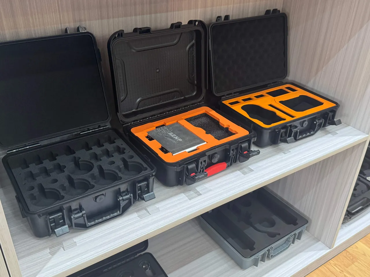
12. Standards Reference: SEMI, ISO 14644 and the ESD Framework
Selection and acceptance of a wafer transport case should be based on the following standards framework.
The SEMI standards. SEMI is the international standards organisation for semiconductor equipment and materials. Its standards cover carrier mechanical interfaces, load ports, kinematic coupling structures, wafer specifications and cleanliness requirements. For 300 mm, the carrier's mechanical interface and door mechanism must match the fab's automated handling system, and the relevant interface dimensions and functional requirements are specified by SEMI standards. When a transport case is used with a standard carrier, its interface design should be consistent with the carrier so that situations such as "the carrier fits in the case but the handling system cannot grip it" or "the stack is unstable" do not arise. SEMI standards also address carrier cleanliness and material requirements, and are an important basis for judging whether carrier and insert materials are acceptable.
The ISO 14644 series. Classification and test methods for cleanrooms and associated controlled environments. ISO 14644-1 provides the method for classifying cleanliness by particle concentration, ISO 14644-2 covers monitoring, and other parts cover design, operation and the cleanliness suitability of various surfaces and materials. The target class for the micro-environment inside a transport case should be determined from the wafer's process stage and customer requirements, not set to the highest possible class across the board.
The ESD framework. ANSI/ESD S20.20 sets requirements for an electrostatic discharge control programme, while IEC 61340-5-1 provides the International Electrotechnical Commission framework for protecting electrostatic-sensitive devices. Together they define material resistance ranges, grounding requirements and handling practice.
Transport test framework. ISTA and GB/T 4857 provide vibration, shock and stacking test methods, while ASTM D4169 builds a performance test sequence based on the distribution cycle. On MIL-STD-810H, the boundary must be stated clearly: in this context MIL-STD-810H is used only as a reference for environmental test methods such as temperature, humidity, vibration and shock. It does not indicate any military certification and does not replace semiconductor cleanliness or static control standards. See MIL-STD-810H environmental testing and case compliance for clarification.
13. Transport Verification: Applying ISTA and GB/T 4857
Wafer transport case verification differs from general industrial packaging in two respects: post-test judgement must be based on particle and cleanliness metrics, and the test must use the actual carrier and correct ballast.
Test design recommendations:
- Sample configuration. Use the real carrier and equivalent wafers (test wafers or ballast wafers) with matching weight, centre of gravity and stiffness. Conclusions from an empty carrier test are not usable.
- Test items. At minimum cover vibration (sine sweep or random), drop (at real handling heights and orientations), stacking (at the real number of layers), and, where applicable, low pressure and temperature-humidity cycling.
- Post-test inspection. Check whether the carrier shifted, whether slots deformed, whether the insert collapsed, and whether the sealing face was damaged; then perform particle counting and visual inspection in a clean environment.
- Acceptance criteria. Agree in advance with the customer or quality department on the maximum permitted particle increase, permitted carrier displacement and permitted insert compression set.
A common mistake is to treat "the case is not broken" as a pass. For wafers, a case that is intact while the carrier moved two millimetres inside may already have generated particles. Judgement criteria must therefore sit at the carrier and wafer level, not the case level.
For test method selection, see ISTA transport test procedures and GB/T 4857 transport packaging testing and case verification. For agreeing a common acceptance criterion with a customer, see ASTM D4169 distribution cycle testing.
14. Pre-Shipment Inspection and Acceptance Points
Pre-shipment checklist:
- Carrier cleaned and particle-confirmed in a clean environment, with records retained
- Wafers correctly located in carrier slots, no tilting, no cross-slotting, no exposure
- Carrier does not move inside the transport case, locating features engaged, plate force appropriate
- Insert free of damage, embedded grit and permanent collapse
- Desiccant fresh and in date, humidity indication normal
- Inerting port, breather valve and pressure equalisation valve functional and unblocked
- Grounding terminal and bonding path intact, bonding resistance within requirement
- Latches, hinges and gaskets in normal condition
- Identification complete: product batch, wafer number range, orientation marks, precautions
- Environmental logger started where fitted
Acceptance sampling points:
| Check item | Method | Acceptance point |
|---|---|---|
| --- | --- | --- |
| Case dimensions and interfaces | Gauges plus trial fit with carrier | Matches carrier and fab interface, no interference |
| Sealing | Water spray or immersion test to the declared IP rating | No leakage, indicator card unchanged |
| Pressure equalisation | Slight positive and negative pressure test | Opening differential within design range, no blockage |
| Grounding continuity | Multimeter measurement of bonding resistance | Resistance from carrier support to grounding terminal within threshold |
| Cleanliness | Wipe sampling plus particle counting | Particle increase within agreed limit |
| Material outgassing | Third-party testing or supplier report | Meets agreed outgassing and ion limits |
| Cushioning performance | Sampled drop or vibration with acceleration measurement | Acceleration peak within the defined threshold |
For volume procurement, introduce an AQL sampling plan and apply tightened sampling to critical characteristics such as cleanliness, sealing, grounding continuity and carrier location. For the methodology, see case acceptance and AQL sampling plans.
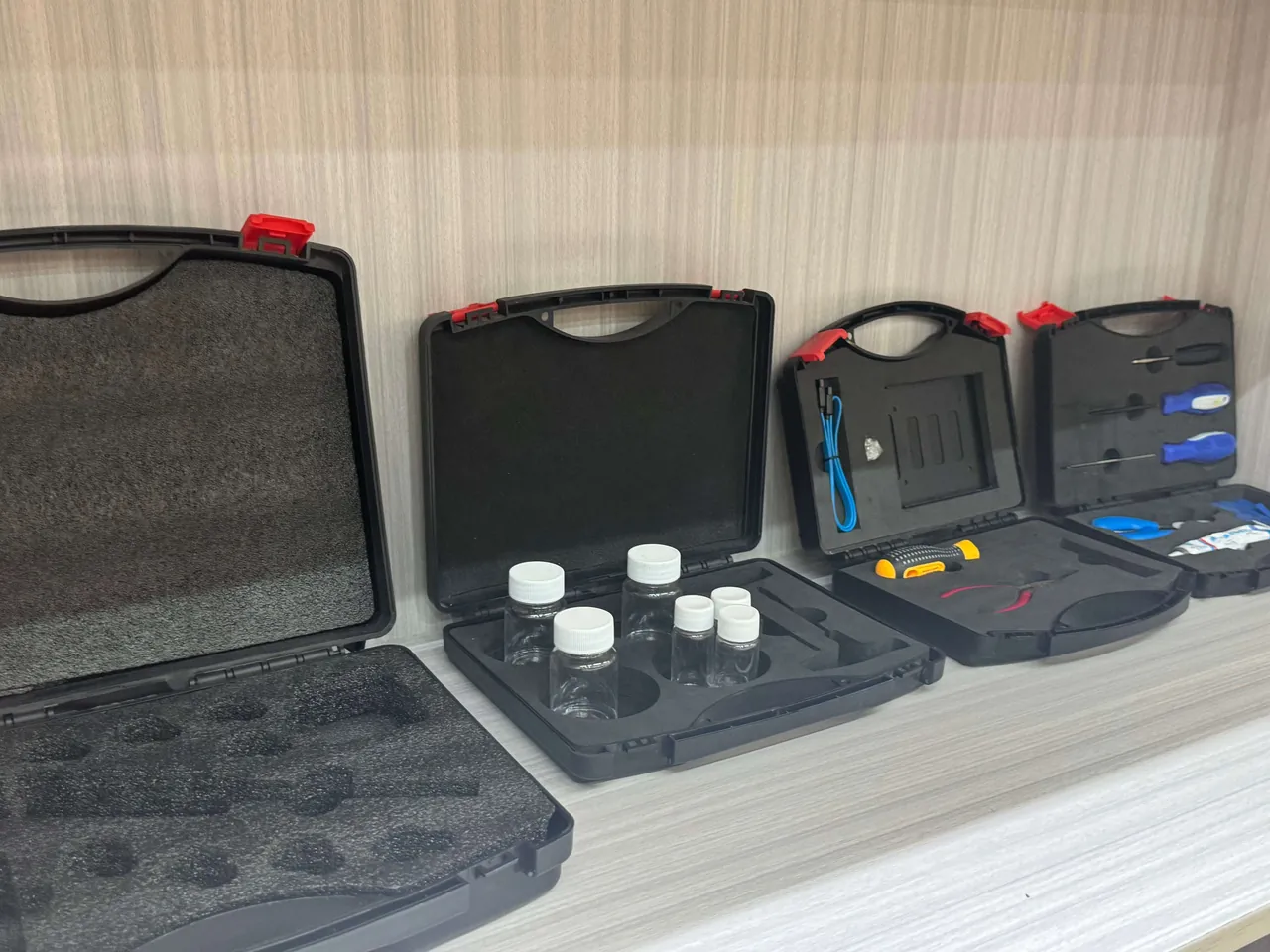
15. Carrier Cleaning, Refurbishment and Life Management
Wafer transport cases are reusable assets, and their performance declines with cycle count.
Cleaning interval and method. Carriers and cases should have a defined cleaning interval, with the actual frequency depending on usage intensity and cleanliness requirements. Cleaning methods must be compatible with the materials: some materials cannot tolerate alcohols or alkaline cleaners, and some gaskets age faster with repeated wiping. Drying and particle confirmation should follow cleaning.
Consumable and wear part management. Latches, hinges, gaskets and pressure equalisation valve membranes are wear parts. Inspection and replacement should be scheduled by cycle count, with spare parts held in stock. For related discussion, see protective case service life assessment and protective case cleaning and maintenance.
Refurbishment and downgrade. When a case shows deformation affecting the sealing face, latch pressure decay or sealing groove damage, options are refurbishment, replacing gaskets, latches and inserts, or downgrading to non-cleanroom use. Cases that already show degraded sealing performance should not continue in service for high-cleanliness wafer transport.
Record management. Each case should have a file recording commissioning date, cumulative cycles, each cleaning and overhaul, and part replacements. This supports both quality management and life or retirement decisions.
16. Common Misconceptions and Engineering Recommendations
Misconception one: "vibration protection means thicker foam." Thicker foam lowers the system natural frequency and, if not handled carefully, brings it closer to the main transport vibration band. The essence of vibration protection is frequency avoidance and damping design, not stacking thickness.
Misconception two: "a higher sealing level means cleaner." High sealing blocks external particles, but outgassing from internal materials and particles generated inside still contaminate wafers, and high sealing amplifies the pressure differential problem. Cleanliness must be assured at the material, cleaning and handling levels together.
Misconception three: "lower humidity is always better." Excessive dryness sharply increases static risk. The humidity target should be set together with static control requirements.
Misconception four: "if the case is not damaged, transport passed." Judgement should be based on carrier displacement, insert deformation and particle increase rather than case appearance.
Misconception five: "any standard carrier fits any case." The carrier's mechanical interface and handling compatibility are specified by SEMI standards, and the way in which a transport case mates with a carrier affects automated handling and stacking stability. This needs dedicated verification.
Summary of engineering recommendations:
- Establish cleanroom compatibility and static control as mandatory gates at the concept stage before discussing structure.
- Document the responsibilities of the carrier and the transport case clearly, and avoid selecting industrial foam for an insert that touches wafers directly.
- Complete ISTA or GB/T 4857 verification with real carriers and equivalent wafers, judging on particle increase and carrier displacement.
- Include gaskets, pressure equalisation valve membranes and inserts in scheduled replacement and life management.
- Select a supplier able to provide matched inserts, seals and pressure equalisation components for the specific carrier model. Through the moulding and tooling capability of Kexin New Materials (Guangdong) Co., Ltd., JUNZHJIA can configure inserts, gaskets and case structures as an integrated package to match customer carrier specifications and cleanliness requirements, supports OEM/ODM and volume supply, and can provide material statements and test documents for customer acceptance.
Frequently Asked Questions
Q: What fundamentally distinguishes a wafer transport case from an ordinary precision instrument case?
A: The difference lies in the acceptance metrics and the failure mechanisms. An ordinary precision instrument case mainly prevents equipment damage from shock, and the acceptance criterion is whether the equipment still functions. In wafer transport, failure typically looks like "the case is intact but the wafer is damaged," and judgement must rest on carrier displacement, insert deformation and particle increase. Wafers are highly sensitive to particles, metal ions, organic outgassing and static, so any contamination originating from case materials, inserts, gaskets or handling can translate into yield loss. In addition, a wafer is a thin plate that responds more to low-amplitude long-duration vibration than to a single impact, which shifts the design objective from shock resistance to micro-vibration and resonance control. Finally, wafer transport normally uses a standard carrier, and the transport case is only one layer of a packaging hierarchy. Its responsibility boundary must be separated clearly from the carrier's, otherwise fundamental errors occur, such as selecting industrial foam for an insert that touches wafers directly.
Q: Is a standard carrier mandatory for 300 mm wafer transport?
A: Yes. From an engineering standpoint this is the only reasonable path. A 300 mm wafer is large in diameter, roughly 775 micrometres thick and high in value, and fabs use fully automated handling systems. The carrier's mechanical interface, door mechanism and locating features must be compatible with the handling system, and the relevant interface dimensions and functional requirements are specified by SEMI standards. The transport case provides shock cushioning, environmental control and traceability on top of the carrier. It does not replace the carrier's job of per-wafer location and clean isolation. If the insert of a transport case touches wafers directly, the insert has effectively been promoted to being a carrier, and it must then meet semiconductor-grade cleanliness and outgassing requirements, which substantially raises both cost and validation effort. The recommended approach is to select a standard carrier compatible with the production line first, then design the insert to match the carrier contour, and validate with physical samples that the carrier does not move inside the case and that the handling system can still grip it correctly.
Q: How should the cleanliness class be set, and is higher always better?
A: Higher is not always better. The target should match the wafer's process stage and customer requirements. ISO 14644-1 classifies cleanliness by particle concentration per unit volume of air, with lower numbers indicating cleaner environments. Critical front-end areas operate at very clean classes, while back-end, metrology and R and D scenarios are less demanding. The micro-environment class inside a transport case should be determined from three inputs: the wafer's current process stage and surface sensitivity, the environments the transport route will expose it to, and the acceptance metrics explicitly defined by the customer or internal quality department. Setting an unnecessarily high class drives cost up rapidly, because materials, cleaning, inspection and packaging layers all need upgrading, while setting it too low introduces uncontrolled yield risk. The recommended approach is to work with quality to translate acceptance requirements into measurable items, such as a maximum particle increase per unit area after opening or a maximum carrier displacement, and then derive the required cleanliness measures from those numbers rather than fixing a class number first.
Q: Why should humidity not be set too low?
A: Because a low-humidity environment significantly increases static accumulation risk, and static is as harmful to wafers as moisture. Electrostatic discharge creates local melt marks on the wafer surface that destroy patterns, and static attracts airborne particles, pinning contaminants onto the wafer that could otherwise be carried away by airflow. When relative humidity drops very low, there is insufficient water vapour in the air to provide a charge drainage path, charge on insulating surfaces dissipates less readily, and discharge risk rises. Humidity control is therefore a balancing problem: higher humidity aggravates metal layer corrosion and water mark formation, while lower humidity aggravates static. In practice the humidity target is set as a band rather than a single extreme value, and it is controlled together with static-dissipative material capability, the grounding path and handling discipline. In no case can material and grounding measures be replaced by humidity control, because humidity only reduces probability and cannot eliminate the discharge condition.
Q: Is a nitrogen purge really necessary for wafer transport?
A: Necessity depends on wafer value, process stage and transport duration. For wafers that have been metallised but not yet packaged, or that require long-term storage or long-distance transport, an inert gas purge reduces internal oxygen content and water vapour partial pressure, suppresses metal layer oxidation and corrosion, and slows the oxidation reactions of organic contaminants. The benefit is clear. For short-distance, short-duration transfers of relatively insensitive wafers, sealing with desiccant is often sufficient, and adding inerting raises the cost of ports, valves and procedures. One point deserves particular attention: inerting does not mean "one fill controls the whole journey." Inert gas also leaks slowly past sealing faces, and the internal-external pressure differential changes with temperature and altitude. If an inerting scheme is adopted, fit a pressure equalisation valve and humidity indication or logging, and read the records before opening as acceptance evidence, rather than equating "was once filled with nitrogen" with "was controlled throughout."
Q: Why is it invalid to verify wafer transport using an empty carrier?
A: Because an empty carrier has completely different mass distribution, centre of gravity and stiffness from a loaded one, so the resulting vibration response, resonance frequencies and shock acceleration peaks are not comparable. The effectiveness of transport protection depends on the dynamic behaviour of the whole system. The case, insert, carrier, rack and wafers together form a multi-degree-of-freedom system. Wafer mass changes the equivalent stiffness and damping, and the presence of wafers in the carrier also changes the carrier's rigidity. Conclusions drawn from an empty carrier test may overestimate or underestimate the protection actually achieved, which makes the verification invalid. The correct approach is to use the real carrier with equivalent wafers, in the form of test wafers or ballast wafers, ensuring matching weight, centre of gravity and stiffness. Loading pattern, retention force and insert configuration should also match the actual shipping state exactly. In addition, post-test judgement should be based on carrier displacement and particle increase rather than only on whether the case was damaged.
Q: How often do the gaskets in a wafer transport case need replacing?
A: There is no single calendar interval. A practical approach is to manage by cycle count plus scheduled inspection, with a time limit as a backstop. Gasket failure appears as cracking, permanent set, hardness change, surface tackiness and embedded particles. Embedded particles are particularly critical in semiconductor applications: even when the gasket body is intact, embedded particles break the continuity of the sealing face, reducing the protection level and potentially becoming a contamination source. A common approach is to set inspection points by cycle count, checking whether the sealing face has embedded grit, whether compression marks fail to recover, and whether cracks are present, while also checking that the sealing groove is clean. On material selection, different elastomers vary widely in their tolerance to cleaning agents, alcohols and ozone, so request a chemical compatibility statement. Because gaskets are low-cost items with a large impact, keep stock on hand and include them in a replacement plan, recording each replacement in the case file.
Q: What is the most commonly overlooked pre-shipment check?
A: Three items are most often overlooked. The first is the state of the case exterior before opening. Many particle problems do not originate inside the case; contamination accumulated on the exterior in an uncontrolled environment is carried into the clean area when the case is opened, so exterior wiping and pass-through window transition must be mandatory steps with records. The second is the actual displacement of the carrier inside the case. Judging by a manual shake that "nothing feels loose" is not reliable; displacement should be controlled by quantified requirements on locating features and plate force, and measured after transport testing. The third is the free flow of the pressure equalisation valve. Once the valve body is blocked by particles or outgassing deposits, the sealed case degenerates into a sealed can and the pressure differential risk returns, yet this condition is completely invisible from the outside. Putting these three items on the pre-shipment checklist as fixed entries, signed off at every shipment, is a practical countermeasure.
Conclusion and Further Reading
The difficulty in designing a wafer transport case is converging five mutually constraining requirements, cleanliness, micro-vibration, static, humidity and pressure, into one deliverable hardware solution. The high value and high sensitivity of wafers means acceptance criteria must rest on carrier displacement, insert deformation and particle increase rather than case appearance. Four disciplines matter in implementation. Establish cleanroom compatibility and static control as mandatory gates at the concept stage. Document the responsibilities of the carrier and transport case clearly, avoiding industrial foam in direct contact with wafers. Complete transport verification with real carriers and equivalent wafers, agreeing acceptance criteria in advance. Include gaskets, pressure equalisation valve membranes and inserts in scheduled replacement and life management.
When selecting a supplier, evaluate three capabilities: whether they can reverse-engineer an insert cavity from carrier specifications and guarantee zero carrier displacement; whether they can provide material statements and test documents meeting cleanliness and low-outgassing requirements; and whether they can integrate pressure equalisation, inerting ports and the grounding path into the case structure. Through the moulding and tooling capability of Kexin New Materials (Guangdong) Co., Ltd., JUNZHJIA provides custom inserts, matched seals, OEM/ODM and volume supply across its protective case, tool case and equipment case product lines, and can support sample builds during the concept validation phase. Above the wafer transport case sit the carrier and production line interfaces, and the companion needs for electronics and equipment protection are covered further in ESD shielding case design and industrial PC and edge computing equipment transport protection.
Further Reading